At the Heart of High-Frequency Technology
They can be used to detect skin cancer, determine the water content of a plant, measure material thickness, or send huge data packets. Terahertz waves are enormous, as are the manufacturing and equipment costs – or they were until now, at least, because Duisburg scientists are working to change that. A tour through the terahertz integration centre.
By Jennifer Meina
Everything from a single source – that’s the goal Dr Nils Weimann and his team have set themselves. The professor of semiconductor technology at the Faculty of Engineering and head of the ‘Components for High Frequency Electronics’ research group is building up Germany’s first terahertz integration centre in collaboration with three UDE colleagues. ‘We form an internationally recognized hub for terahertz research together with other network partners, especially from North Rhine-Westphalia.’ One advantage of the location is that the entire technology chain is located here, from the manufacture of semiconductor material and the production of chips to the production of modules and special terahertz measuring technologies. More than seven million euros in state and EU funding is flowing into the Centre for Semiconductor Technology and Optoelectronics (ZHO) in Duisburg. ‘Terahertz waves will provide more capacity in future mobile communications networks – the keyword is 6G. But the technology is capable of much more than just transferring hundreds of gigabits per second,’ stresses Weimann. ‘It also enables robots and machines to determine the exact position of objects and simultaneously to learn something about their material properties, in what we call “communication and sensing” in future wireless networks. Terahertz waves have enormous potential.’
1. MATERIALS SYNTHESIS: MAKING A CIRCUIT OUT OF GAS
Terahertz waves are electromagnetic waves that lie between infrared radiation and microwaves. But unlike for its ‘neighbours’ with smaller or larger frequencies, there is as yet no chip technology for terahertz waves capable of processing this radiation efficiently and thus inexpensively. The Duisburg scientists want to change that.
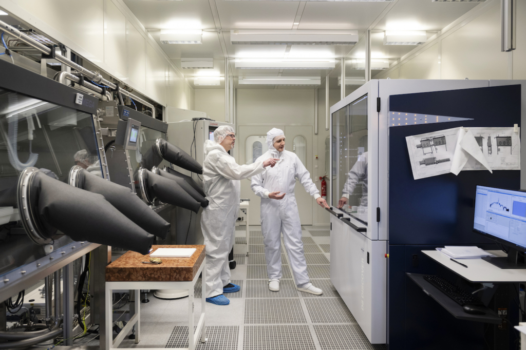
Semiconductor production starts in the ZHO cleanrooms – or more precisely, in the epitaxy system operated by doctoral candidate Alexander Poßberg (picture 1). Here, a wafer made of indium phosphide is inserted. ‘Wafers in chip technology are usually made of silicon, but our semiconductor material is better suited to ultra-high frequencies,’ explains Weimann. These wafers are the foundation, the base of the chips, which are created hundreds of times on a single wafer. Special crystal layers are applied to the ultra-fine, round disc, which is about the size of the palm of a hand, in a method known as epitaxy. In the process, a gas that is initially mixed individually is passed over the wafer (picture 2). Under the influence of heat, the gas decomposes into individual atoms that are deposited – layer by layer, in perfect alignment – onto the wafer. The crystal’s composition can be adjusted via the concentration of the molecules in the gas stream. This is all controlled by computer.
The wafer now consists of more than 30 layers of different materials, several of which are just a few nanometres thick (picture 3).
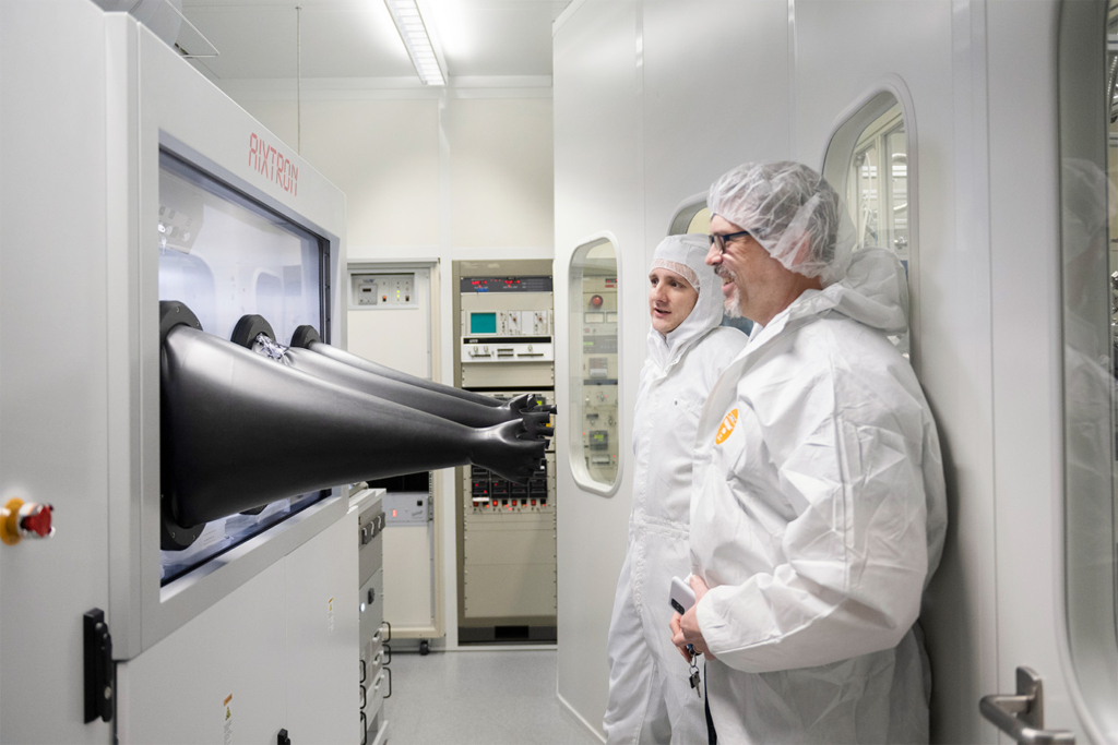
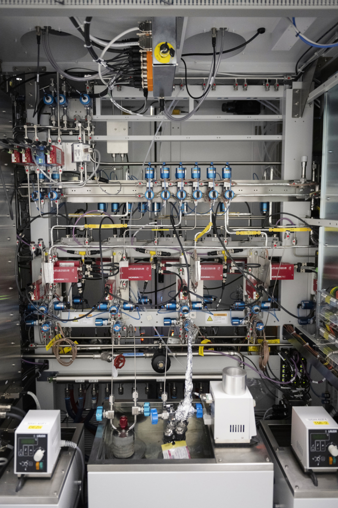
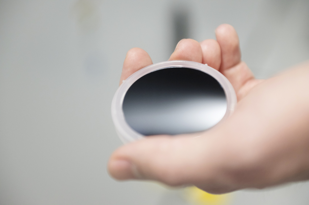
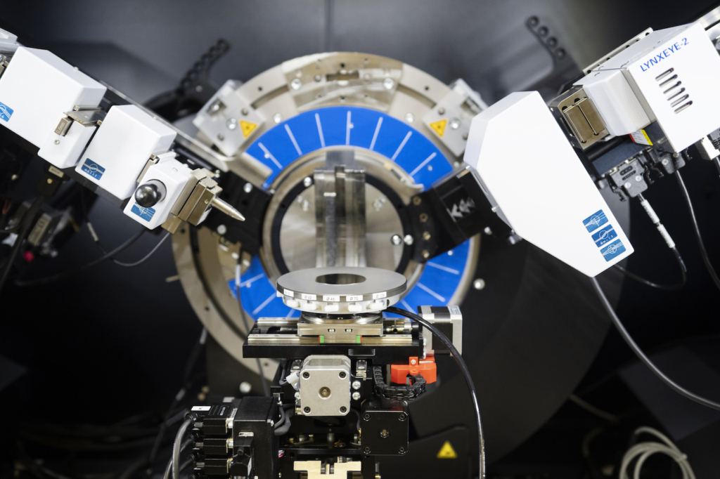
How suitable is this composition as a starting material for semiconductor devices? This is analysed in the X-ray diffractometer (picture 4). This method measures the distances between the atoms and the thickness of the individual layers to one interatomic distance.
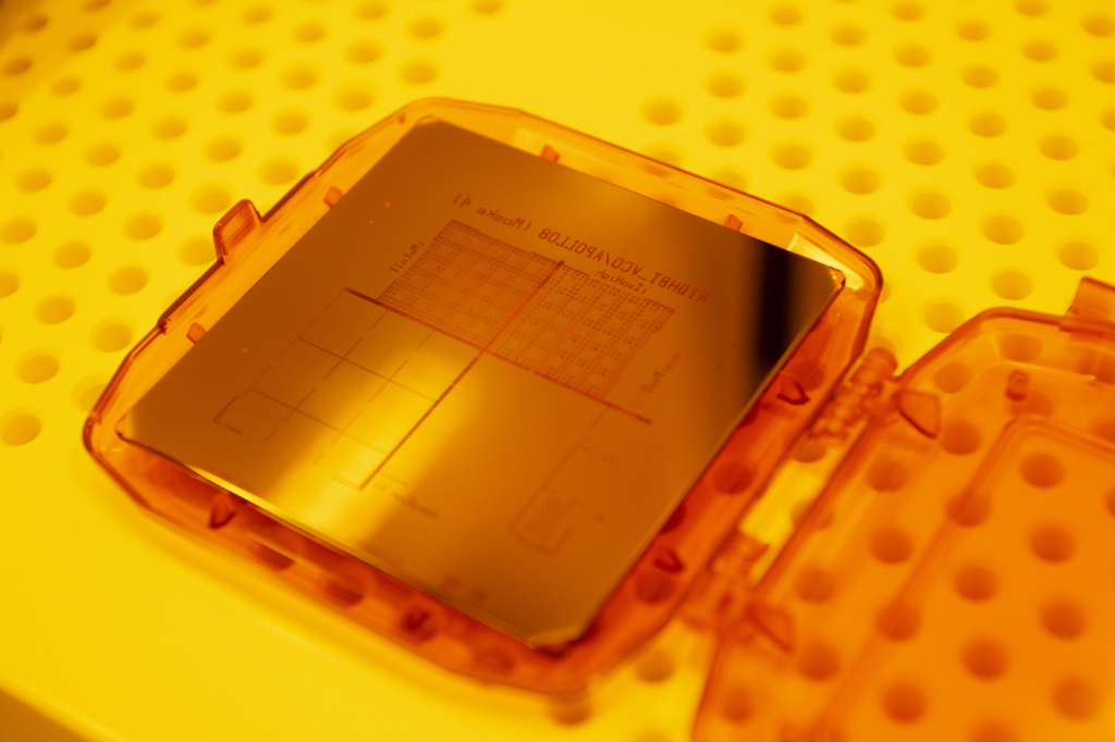
If the results of the analysis are promising, the next step is to create microscopic structures on the wafer surface via photolithography. This involves applying a light-sensitive layer to the wafers and then exposing it through various photomasks (picture 5). The masks consist of glass with a layer of chrome, in which openings are made. With this method, a structre can be repeated on any number of wafers in a manner similar to lithography, known from letterpress printing. It takes 10 to 20 production steps to create the structure on the wafer needed to isolate individual components via etching processes and provide them with metal contacts. With UV exposure, it is possible in this way to produce structures of around one micrometre in size – one hundredth of the diameter of a hair. ‘But we can even go a hundred times smaller: With our new electron beam lithography, we can define structures with a size of less than ten nanometres. That’s about 25 interatomic distances in the crystal or one ten-thousandth of the diameter of a strand of hair,’ says Weimann.
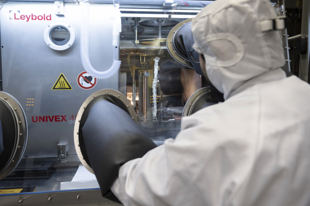
Directly opposite the X-ray machine (picture 6) the researchers are looking at is the custom-built metal coating system (l.), into which the wafer pieces are placed. As the oxygen in the air interferes with the process, scientists like PhD student Enes Mutlu can only in reach into the installation with the help of integrated gloves (picture 7). In the vacuum chamber, metal is evaporated and lands on the surface of the wafer, forming a thin layer – creating current-conducting contacts.
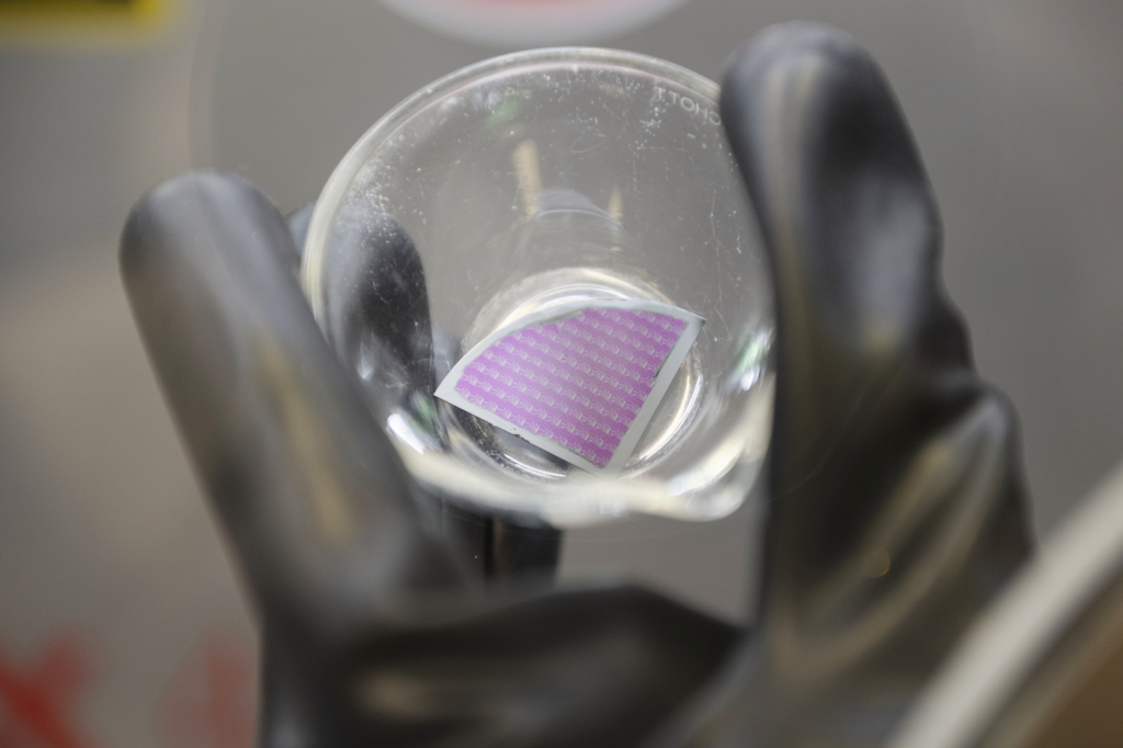
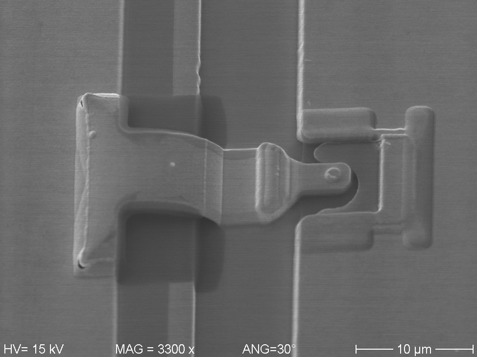
At the end of wafer fabrication, the wafer discs are sawed into tiny chips, which measure only a few millimetres on the side. Each chip contains a terahertz transmitter or receiver with integrated antennae (picture 8). A single transmitter is only visible under a microscope (picture 9).
2. MEASUREMENT: APPLYING TENSION
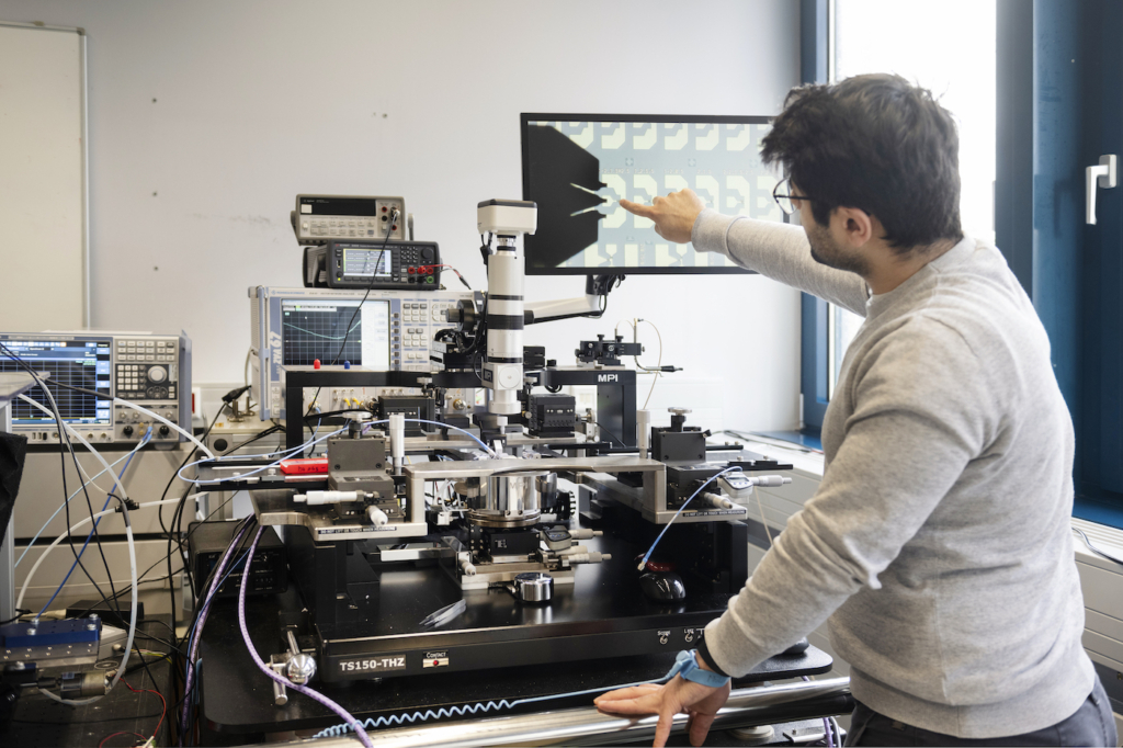
The scientists determine whether the production process was successful in an electrical function test. Ultra-fine needles are placed on the chip’s surface under 10,000-fold magnification, and special measuring instruments are used to check the emission of terahertz waves (picture 10).
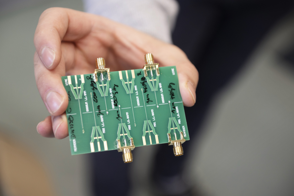
The tiny chips are mounted on circuit boards for integration into larger measurement setups, allowing applications such as the inspection of paint thickness in automobile manufacturing or research on the water balance of plants. One has to look closely with the naked eye to see the chip within the larger assembly: they are the miniscule golden squares on the line in the middle of the circuit board (picture 11).
3. MODULE PRODUCTION: NOT READY-MADE
The circuit boards (picture 11) are well suited for nearfield exploration, such as integration into instruments that can be used to visualise the skin’s surface. Terahertz is well suited for medical and biological applications as the radiation does not cause any damage to tissues.
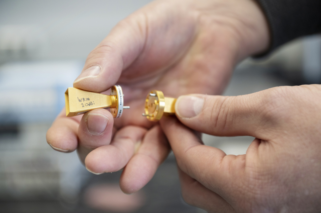
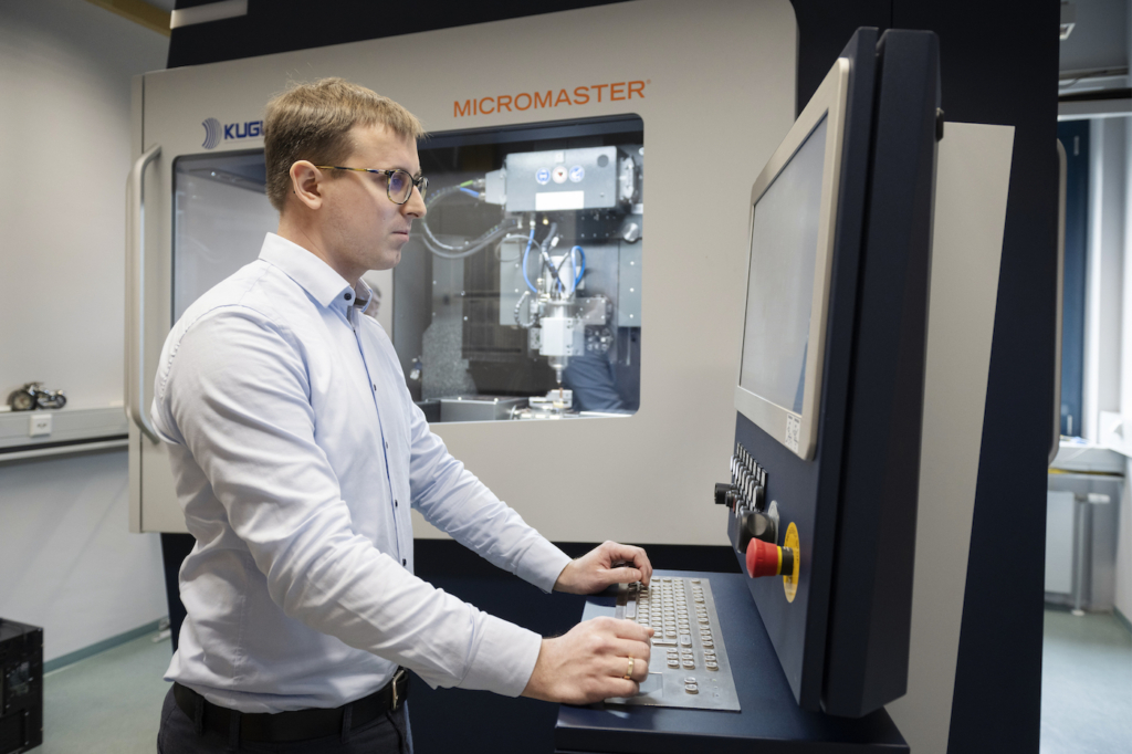
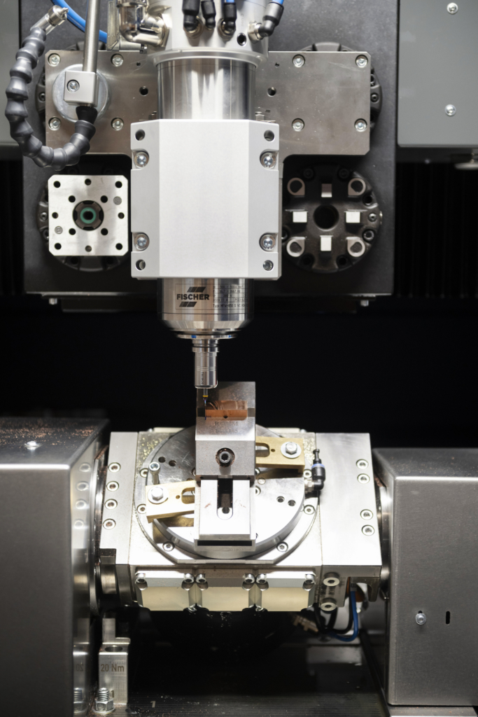
To cover further distances, special terahertz modules are required (picture 12). A terahertz system currently costs as much as a luxury car – around 50,000 to 100,000 euros – and is the size of a refrigerator. In the future, the transmitters and receivers will become not only considerably less expensive – only a few hundred euros – but also much more energy-efficient and several times smaller. In the UDE modules, the terahertz waves are directed into air channels half a millimetre wide and high. The channels are enclosed with metal on all sides, like a rectangular pipe. A terahertz module combines the signals of several chips via such channels, which provides more transmit power and also enables directional control of the terahertz beams exiting the module. The channels are cut into the metal with great precision, with an accuracy to within a micrometre. This requires a special milling machine that is not just state of the art but also found exclusively at UDE (picture 13).
Here, PhD student Konrad Müller can now create the desired model of the module by means of a 3D plan and implement it in the milling machine (picture 14). ‘The microprecision milling machine can make narrow trenches 100 to 300 micrometres wide in metal blocks. That’s the width of one to three strands of hair,’ explains Weimann.
After the trenches have been precisely milled, they are sealed with a metal lid, creating the narrow channels, also known as waveguides, in which the terahertz waves are guided between the semiconductor chips and to the antenna – this is the end product, a terahertz module, which can be integrated in measurement or communication systems.
The UDE team is still in the research phase; the path to market maturity is still long. Weimann estimates that the efficient terahertz chip technology under development here will be ready for use in industry in around five to ten years. ‘Terahertz is a large part of the entire electromagnetic spectrum, but it is hardly used due to a lack of components. Terahertz waves do not damage living tissue, can transmit large amounts of data, and distinguish between material surfaces. Their short length also enables the use of small antennae. In combination, these properties result in many new applications, including some that do not yet appear on our radar.’
This is a big topic: the DFG collaborative research centre MARIE, the BMBF network 6G-HUB 6GEM, and the NRW research network terahertz.nrw are all working on terahertz applications based on technologies which are now being developed in Duisburg.
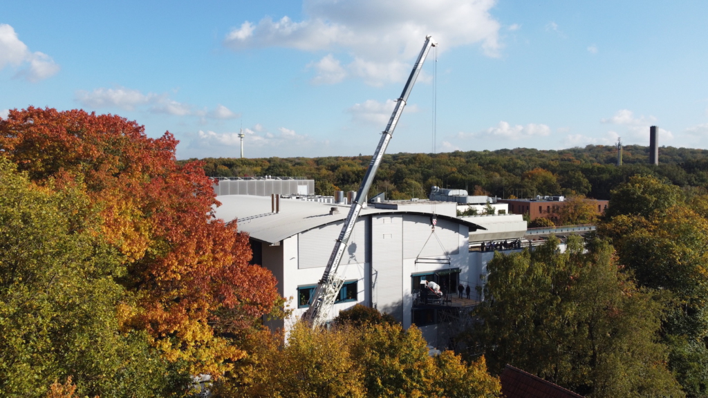
The milling machine was custom made to the specifications of the UDE researchers. And in October 2022 it was delivered to the ZHO at a dizzying height: Since the approximately 3m³ large and four tonne heavy milling machine did not fit in the elevator, a crane lifted it directly into the room – through a hole in the building wall.
Main image: © Bettina Engel-Albustin


